MIC184
Micrel
MIC184
4
May 2006
Symbol
Parameter
Condition
Min
Typ
Max Units
Serial Data I/O Pin (DATA)
V
OL
Low Output Voltage
I
OL
= 3mA
0.4
V
I
OL
= 6mA
0.8
V
V
IL
Low Input Voltage
2.7V d V
DD
d 5.5V
0.3V
DD
V
V
IH
High Input Voltage
2.7V d V
DD
d 5.5V
0.7V
DD
V
C
IN
Input Capacitance
10
pF
I
LEAK
Input current
?.01
?
礎
Serial Clock Input (CLK)
V
IL
Low Input Voltage
2.7V d V
DD
d 5.5V
0.3V
DD
V
V
IH
High Input Voltage
2.7V d V
DD
d 5.5V
0.7V
DD
V
C
IN
Input Capacitance
10
pF
I
LEAK
Input current
?.01
?
礎
Status Output (INT)
V
OL
Low Output Voltage,
I
OL
= 3mA
0.4
V
Note 8
I
OL
= 6mA
0.8
V
t
INT
Interrupt Propagation Delay,
from TEMP > T_SET, FQ = 00 to INT < V
OL
,
t
CONV
+1 ?/SPAN>s
Note 5
R
PULLUP
= 10k? POL bit = 0
t
nINT
Interrupt Reset Propagation Delay,
from any register read to INT > VOH,
1
祍
Note 5
R
PULLUP
= 10k? POL bit = 0
T_SET
Default T_SET Value
t
POR
after V
DD
> V
POR
, Note 9
80
80
80
癈
HYST
Default HYST Value
t
POR
after V
DD
> V
POR
, Note 9
75
75
75
癈
Serial Interface Timing (Note 5)
t
1
CLK (Clock) Period
2.5
祍
t
2
Data In Setup Time to CLK High
100
ns
t
3
Data Out Stable After CLK Low
0
ns
t
4
DATA Low Setup Time to CLK Low
start condition
100
ns
t
5
DATA High Hold Time
stop condition
100
ns
After CLK High
Note 1. Exceeding the absolute maximum rating may damage the device.
Note 2. The device is not guaranteed to function outside its operating rating.
Note 3. Devices are ESD sensitive. Handling precautions recommended.
Human body model: 1.5k in series with 100pF. Machine model: 200pF, no series resistance.
Note 4. Final test on outgoing product is performed at T
A
= TBD癈.
Note 5. Guaranteed by design over the operating temperature range. Not 100% production tested.
Note 6. Accuracy specication does not include quantization noise, which may be as great as ?/SPAN>
1
D2LSB (?/DIV>
1
D4癈).
Note 7. T
D
is the temperature of the remote diode junction. Testing is performed using a single unit of one of the transistors listed in Table 5.
Note 8. Current into the INT pin will result in self-heating of the MIC184. INT pin current should be minimized for best accuracy.
Note 9. This is the decimal representation of a binary data value.
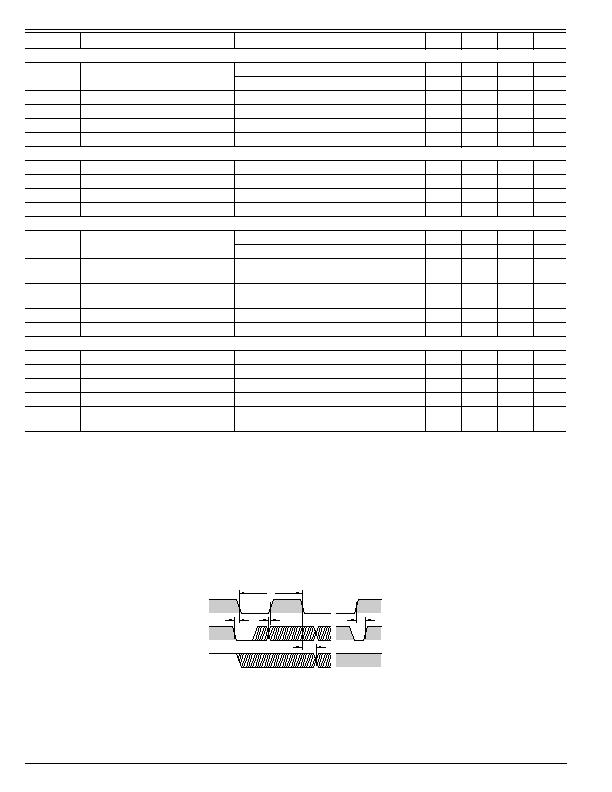
Timing Diagram
t
1
t
2
t
5
t
4
t
3
SCL
SDA Input
SDA Output
Serial Interface Timing
发布紧急采购,3分钟左右您将得到回复。
相关PDF资料
MIC2086-MBQS TR
IC CTRLR HOW SWAP SGL 20-QSOP
MIC2225-4OYMT TR
IC REG DL BUCK/LINEAR 10TMLF
MIC2310-2ZTS TR
IC HOT SWAP CTLR 2CHAN 24TSSOP
MIC2341-2YTQ
IC HOT PLUG CTLR DUAL PCI 48TQFP
MIC2569YQS TR
IC POWER SWITCH CABLECARD 16QSOP
MIC2583R-MBQS TR
IC CTRLR HOT SWAP 200MV 16-QSOP
MIC2585-2MBTS TR
IC CTRLR HOT SWAP DUAL 24-TSSOP
MIC2586R-2BM TR
IC CTRLR/SEQ HOT SWAP 14-SOIC
相关代理商/技术参数
MIC184BMM
功能描述:IC SUPERVISOR LOCAL/REMOTE 8MSOP RoHS:否 类别:集成电路 (IC) >> PMIC - 热管理 系列:- 标准包装:2,500 系列:SilentSense™ 功能:温度监控系统(传感器) 传感器类型:内部和外部 感应温度:-55°C ~ 125°C,外部传感器 精确度:±2°C 本地(最大),±3°C 远程(最大) 拓扑:ADC(三角积分型),比较器,寄存器库 输出类型:I²C?/SMBus? 输出警报:是 输出风扇:是 电源电压:2.7 V ~ 5.5 V 工作温度:-55°C ~ 125°C 安装类型:表面贴装 封装/外壳:8-TSSOP,8-MSOP(0.118",3.00mm 宽) 供应商设备封装:8-MSOP 包装:带卷 (TR) 其它名称:MIC284-2BMMTRMIC284-2BMMTR-ND
MIC184BMM TR
功能描述:IC SUPERVISOR LOCAL/REMOTE 8MSOP RoHS:否 类别:集成电路 (IC) >> PMIC - 热管理 系列:- 标准包装:2,500 系列:SilentSense™ 功能:温度监控系统(传感器) 传感器类型:内部和外部 感应温度:-55°C ~ 125°C,外部传感器 精确度:±2°C 本地(最大),±3°C 远程(最大) 拓扑:ADC(三角积分型),比较器,寄存器库 输出类型:I²C?/SMBus? 输出警报:是 输出风扇:是 电源电压:2.7 V ~ 5.5 V 工作温度:-55°C ~ 125°C 安装类型:表面贴装 封装/外壳:8-TSSOP,8-MSOP(0.118",3.00mm 宽) 供应商设备封装:8-MSOP 包装:带卷 (TR) 其它名称:MIC284-2BMMTRMIC284-2BMMTR-ND
MIC184YM
功能描述:板上安装温度传感器 Improved LM75 Series Local/Remote Temperature Sensor in SOIC-8 Lead-Free
RoHS:否 制造商:Omron Electronics 输出类型:Digital 配置: 准确性:+/- 1.5 C, +/- 3 C 温度阈值: 数字输出 - 总线接口:2-Wire, I2C, SMBus 电源电压-最大:5.5 V 电源电压-最小:4.5 V 最大工作温度:+ 50 C 最小工作温度:0 C 关闭: 安装风格: 封装 / 箱体: 设备功能:Temperature and Humidity Sensor
MIC184YM TR
功能描述:板上安装温度传感器 Improved LM75 Series Local/Remote Temperature Sensor in SOIC-8 Lead-Free
RoHS:否 制造商:Omron Electronics 输出类型:Digital 配置: 准确性:+/- 1.5 C, +/- 3 C 温度阈值: 数字输出 - 总线接口:2-Wire, I2C, SMBus 电源电压-最大:5.5 V 电源电压-最小:4.5 V 最大工作温度:+ 50 C 最小工作温度:0 C 关闭: 安装风格: 封装 / 箱体: 设备功能:Temperature and Humidity Sensor
MIC184YMM
功能描述:板上安装温度传感器 Improved LM75 Series Local/Remote Temperature Sensor in MSOP-8 Lead-Free
RoHS:否 制造商:Omron Electronics 输出类型:Digital 配置: 准确性:+/- 1.5 C, +/- 3 C 温度阈值: 数字输出 - 总线接口:2-Wire, I2C, SMBus 电源电压-最大:5.5 V 电源电压-最小:4.5 V 最大工作温度:+ 50 C 最小工作温度:0 C 关闭: 安装风格: 封装 / 箱体: 设备功能:Temperature and Humidity Sensor
MIC184YMM TR
功能描述:板上安装温度传感器 Improved LM75 Series Local/Remote Temperature Sensor in MSOP-8 Lead-Free
RoHS:否 制造商:Omron Electronics 输出类型:Digital 配置: 准确性:+/- 1.5 C, +/- 3 C 温度阈值: 数字输出 - 总线接口:2-Wire, I2C, SMBus 电源电压-最大:5.5 V 电源电压-最小:4.5 V 最大工作温度:+ 50 C 最小工作温度:0 C 关闭: 安装风格: 封装 / 箱体: 设备功能:Temperature and Humidity Sensor
MIC196
制造商:American DJ 功能描述:Laser Light Effect DMX Red Green and Blue Laser
MIC1R
制造商:Velleman Inc 功能描述:
